Projects
Selected engineering and academic projects
Integrating native BRAM Controller and Display SPI MASTER via AXI4-Lite for PS–PL Communication
In Progress
Sep 2026 – Present
Project Overview
Currently integrating previously developed native BRAM controller and SPI Master on OLED Controller IC into a Zynq-based PS–PL system using AXI4-Lite communication. The goal is to allow software(Vitis) running on the processing system (PS) to control custom RTL modules implemented in programmable logic (PL) through memory-mapped AXI interfaces.
Unlike the earlier training project, this personal project was rebuilt independently using an Arty Z7-10 Zynq board and an SH1106 128×64 OLED display. I first implemented and tested the native BRAM controller and SPI OLED master separately, then began integrating them into a single PS–PL system. Some portions of the RTL were also refined with the help of AI to improve code organization and make the implementation closer to common industry-style RTL practices.
Useful RTL Design Techniques Learned
-
Rising-edge detection for control inputs
assign a_rise = a & ~a_prev;By comparing the current value of a signal with its previous value, a one-cycle pulse can be generated when a rising edge occurs. This is useful for converting a level-based input into a one-cycle control event, such as a start pulse. For asynchronous external inputs, this technique can be used after a two-flop synchronizer, which helps reduce metastability risk before edge detection.
-
Parameterized SPI serial-clock generation
localparam integer HALF_DIV_RAW = CLK_HZ / (SPI_HZ * 2);

localparam integer HALF_DIV =
    (HALF_DIV_RAW < 1) ? 1 : HALF_DIV_RAW;
Together with logic such as:
if (divider_count >= HALF_DIV - 1)The SPI serial clock (SCLK) can be generated by dividing the FPGA system clock using a configurable half-period counter. The divider value is calculated as HALF_DIV = f_sys / (2 × f_SCLK), which represents the number of FPGA system clock cycles in one half-period of SCLK. Toggling SCLK every HALF_DIV system clock cycles produces the desired SPI clock frequency in a clean and parameterized manner.
-
Start / Busy / Done transaction control
Introducing explicit
start,busy, anddonesignals made the SPI master interface more organized. A start pulse begins a transaction, busy indicates that transmission is in progress, and done provides a clear indication that the complete SPI transaction has finished. This separates transaction-level control from individual SCLK transitions. -
Bit-index-based grouped transmission
A decrementing
bit_indexcounter provides a clean way to track which bit is currently being transmitted through MOSI. This makes each byte or command transaction easier to organize, and allows the controller to clearly detect when a complete group of bits has been transmitted. -
Explicit SPI edge behavior
The SPI transfer logic was organized around the behavior of the serial-clock edges. In the SPI mode used for the OLED interface, MOSI is kept stable so that the OLED can sample the current bit on the rising edge of SCLK, while the falling edge is used to shift or prepare the next MOSI bit. This made the relationship between the shift register, MOSI output, and serial-clock timing much easier to understand and debug.
Semiconductor RTL Design Intensive Training Program
Completed
Jun 2026 – Jul 2026
1. Introduction
This was a mission-based intensive RTL and FPGA design training program focused on developing fundamental digital design and SoC implementation skills.
For each mission, only the required specifications, interface requirements, and relevant datasheets were provided. I independently developed the RTL architecture from the initial design concept, implemented the design in Verilog, and verified it on FPGA hardware. Because the designs were developed independently without pre-built RTL solutions, the process involved substantial hands-on trial and error, allowing me to encounter and resolve practical design and debugging issues firsthand.
The missions progressed from fundamental RTL and finite-state-machine design to peripheral communication, AMBA bus protocols, memory interfaces, and Zynq PS–PL integration, providing a practical foundation in FPGA-based SoC design.
2. Technical Scope
- Verilog RTL Design
- Finite State Machine (FSM) Design
- FPGA Synthesis and Implementation
- SPI MASTER Peripheral Controller Design
- AMBA APB3 Protocol and Custom Slave IP
- AXI-Based Zynq PS–PL Integration
- Block RAM (BRAM) Interface Design
- Vivado ILA Hardware Debugging
- Bare-Metal C with Vitis
- Datasheet-Driven Hardware Development
3. Mission I — FPGA RTL Fundamentals
Four-Way Traffic Light Controller
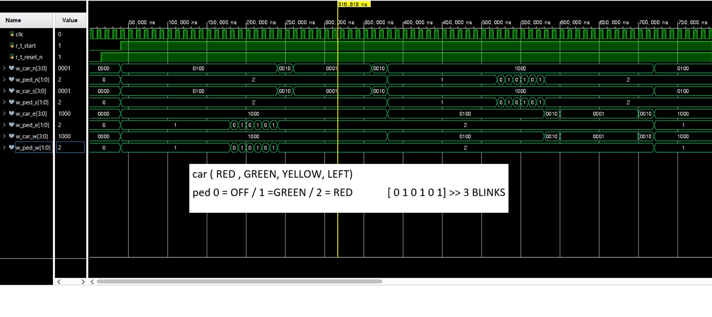
Designed a four-way traffic-light controller using a finite state machine, including left-turn vehicle signals and pedestrian signals. Implemented clock division, RTL control logic, XDC pin constraints, FPGA bitstream generation, and on-board verification.
Technical Challenges & Debugging
- Minor debugging was required when merging four one-way traffic-light FSM modules into one top module, including internal wiring and proper wire-type declarations.
- After creating the first HDL draft, I realized that the design was operating directly from the system clock rather than using a one-second timing period. I therefore scaled the clock to a one-second period and implemented LED flickering using an additional registered timing signal.
- Since this was my first mission involving board implementation, I initially struggled to find the correct XDC reference information and match the FPGA pins. It took a substantial amount of time to extract the necessary information from the datasheets and board schematics.
Mission Demonstration
Implementation & Verification Materials
Design Notes


Source Code
4. Mission II — SPI Peripheral Controller
MCP3004 ADC Interface
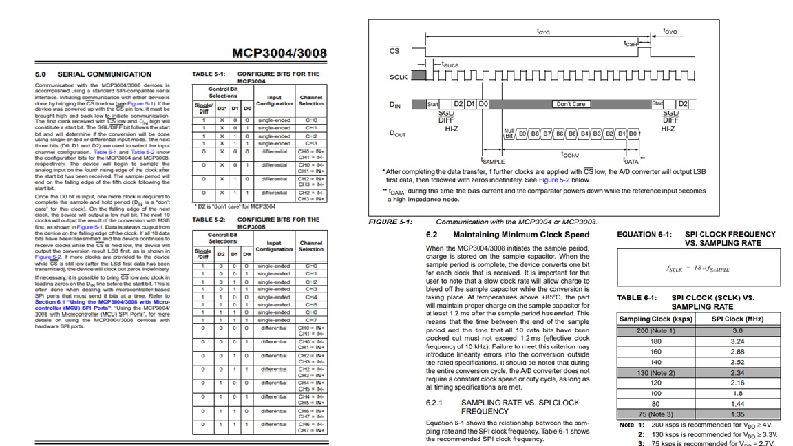
Developed an SPI master to sequentially acquire ADC data from three photoresistors through an MCP3004 and implemented calibrated LED activation thresholds. SPI timing and ADC transactions were verified using Vivado ILA.
Technical Challenges & Debugging
- Since the main materials provided were the MCP3004 datasheet and board schematic, I had to independently determine how the SPI master transaction worked and how the MCP3004 communicated with the master IP.
- Because three photoresistors produced analog inputs simultaneously, one challenge was determining how to organize ADC acquisition inside the FSM. I implemented sequential access through Channel 0, Channel 1, and Channel 2.
- Determining and generating the appropriate SPI serial-clock timing was another challenge during the implementation.
Mission Demonstration
Implementation & Verification Materials
Design Notes

Source Code
5. Mission III — AMBA APB3 Slave IP
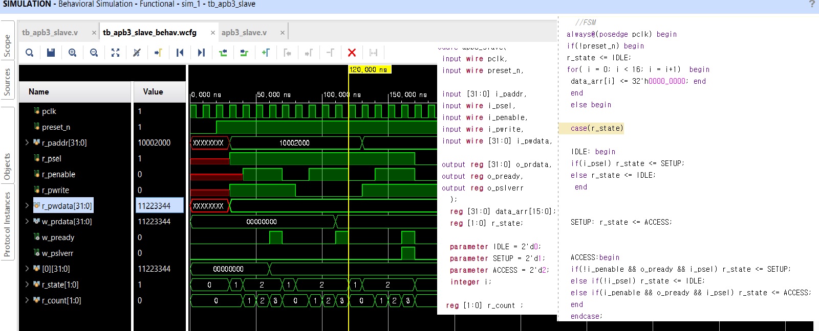
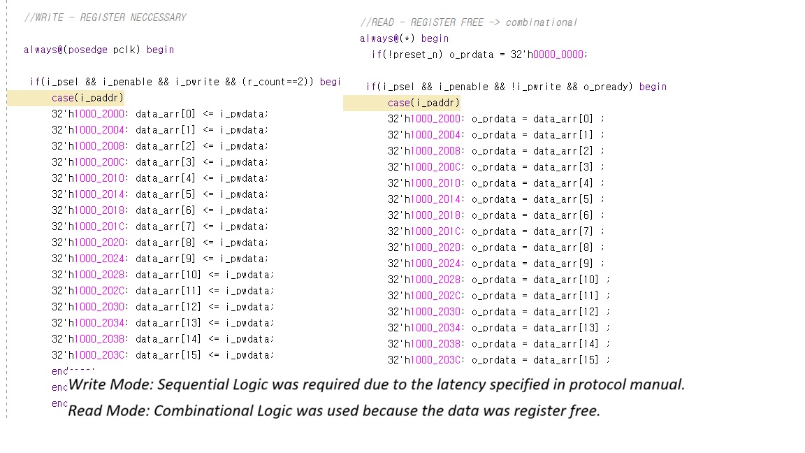
Studied APB3 transaction phases and implemented a custom register-mapped APB3 slave for a 64-byte address space starting at 0x1000_0000. The design was verified using an APB master testbench.
Technical Challenges & Debugging
- Analyzing the interface scenario using the AMBA specification document was the most challenging part of this mission. Distinguishing the requester and completer roles helped me understand how communication occurs between the master and slave.
- Mapping the 64-byte address space into sixteen 32-bit registers was another design consideration when creating the FSM and register-access logic.
Mission Demonstration

Implementation & Verification Materials
Design Notes
Source Code
6. Mission IV — Zynq PS–PL Integration
Configured the ARM Cortex-A9 processing system and executed bare-metal software through Vitis. Verified UART communication and implemented an interrupt-driven LED controller using AXI GPIO and the Zynq Generic Interrupt Controller.
Technical Challenges & Debugging
- The mission required an interrupt-based LED controller using AXI GPIO. Since I had no previous experience with software drivers, I first generated the hardware block design, exported the bitstream to Vitis, and studied relevant example code.
- I analyzed header files and APIs related to GPIO and interrupt handling, including how the XGpio and ScuGic instances are initialized and how interrupt handlers interact with the hardware.
- After understanding the signal and software path from Button → AXI GPIO → GIC → CPU → Handler, I adapted the example structure into my own LED-controller implementation.
Mission Demonstration
Design Notes
Source Code
7. Mission V — PS-Side BRAM Access
Built an AXI-connected BRAM subsystem and performed a 256-word write/read memory-integrity test from bare-metal C running on the Zynq processing system.
Technical Challenges & Debugging
- Initially, I expected the BRAM controller to use a software-driver instance similar to the previous AXI GPIO mission. However, after reviewing the generated platform code and available examples, I found that direct memory-access macros were used instead.
- This led me to Xil_IO functions and memory-mapped read/write operations, which helped me understand that the BRAM controller did not require a separate software-driver instance for normal memory access.
- Since the data width was 32 bits, I also had to ensure that addresses were aligned according to 4-byte memory-access boundaries.
Mission Demonstration
Design Notes
Source Code
8. Mission VI — PL-Side BRAM Controller
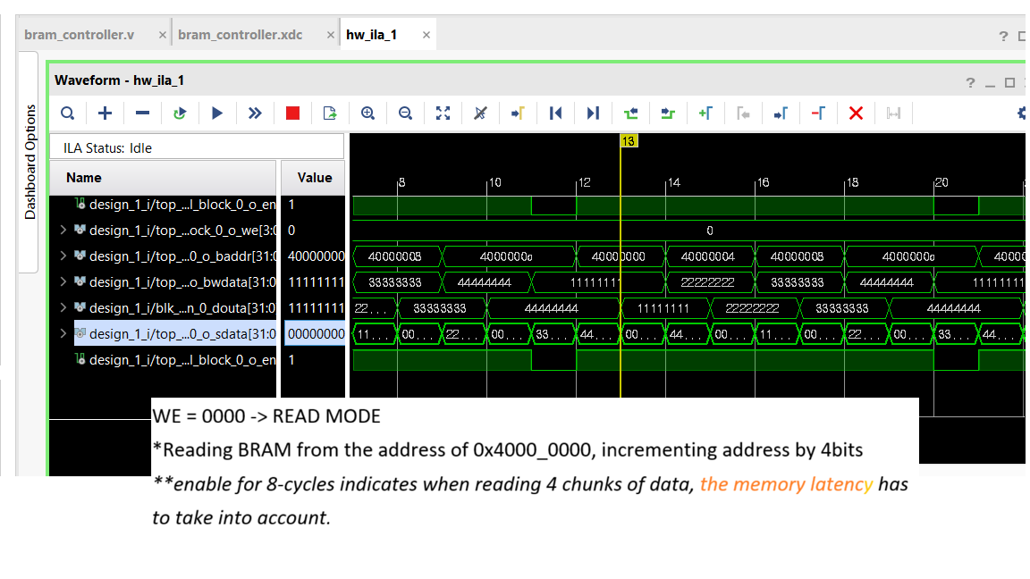
Designed a custom BRAM controller in Verilog, packaged the module as Vivado IP, and verified native BRAM read/write transactions using Vivado ILA.
Technical Challenges & Debugging
Debugged reset polarity, clock connectivity, write-enable timing, and BRAM read latency by observing internal control and data signals through Vivado ILA.
Implementation & Verification Materials
Design Notes
Source Code
9. Mission VII — SPI OLED Controller
Implemented a 4-wire SPI controller for an SSD1315 OLED display, including display initialization, command/data control, reset sequencing, and FPGA-based hardware verification.
Technical Challenges & Debugging
Debugging focused on the OLED initialization sequence, reset timing, SPI transaction boundaries, command/data selection, and display-memory addressing required by the device.
Mission Demonstration
Design Notes
Source Code
10. Training Reflection
A substantial amount of inference and analysis was required because I did not have a strong background in RTL or FPGA design when I began this training. Through the progression of the missions, I became more confident in my ability to learn unfamiliar technical concepts and translate hardware specifications and peripheral datasheets into RTL architectures and working Verilog implementations.
The project-based process also taught me that perfection is not always the best engineering strategy. Spending too much time trying to make an initial design perfect can leave less time and energy for implementation and debugging. I therefore learned to approach initial designs more directly, verify them incrementally, and improve them through debugging.
This training also gave me a broader perspective on electrical engineering and semiconductor systems. My previous interests were more focused on analog semiconductor devices, but working with FPGA-based digital systems helped me better understand how interfaces, controllers, memories, processing systems, and other hardware blocks interact within a complete system.
11. Training Outcome
Through these missions, I became much more familiar with register-based systems, including how registers work with addresses and how different I/O protocols communicate with peripherals.
Without relying mainly on textbooks or lectures, I learned many of these concepts directly through the projects by searching how each protocol works and applying the specifications to my own designs. This helped me build a more practical understanding of computer architecture and how different hardware blocks communicate with each other.
I also became more comfortable working with datasheets. As I worked with new devices and protocols, I learned how to find timing requirements, register information, initialization sequences, and other specifications from unfamiliar technical documents and use them in actual RTL implementations.
Overall, the training lowered the barrier to approaching unfamiliar hardware, protocols, and technical documentation, while giving me a practical foundation for more complex FPGA-based SoC and hardware-accelerator projects.
Project Materials
MOSFET Physics and SONOS Memory Analysis using Sentaurus TCAD
Completed
May 2026
1. Introduction
This project focuses on understanding Synopsys Sentaurus TCAD simulation. The main objective was to simulate semiconductor devices in a virtual environment and visualize their electrical and physical behavior by adjusting device parameters and command code. Through numerical simulation, MOSFET operation, short-channel effects (SCE), device optimization techniques, and SONOS memory operation were investigated. This project connected theoretical semiconductor concepts with practical device simulation and visualization.
2. TCAD Workflow
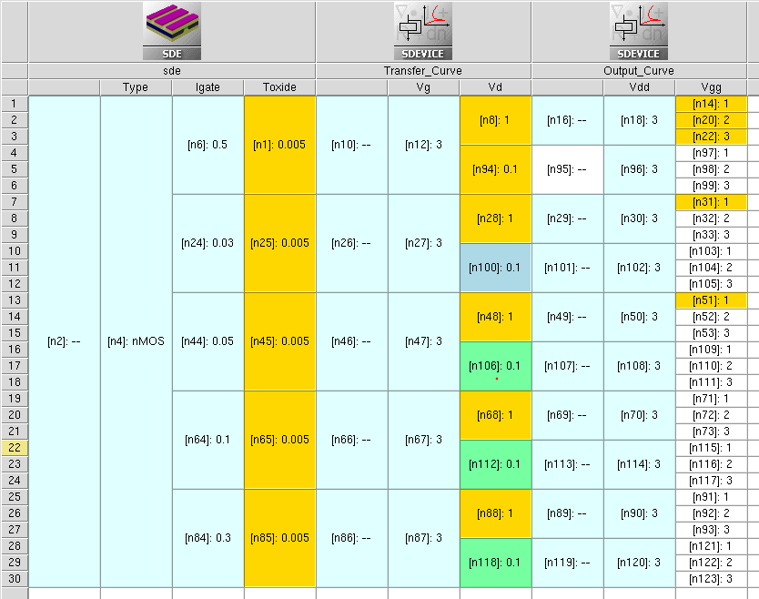
Sentaurus Workbench was used to organize the simulation flow. Device structures were created in Sentaurus Structure Editor (SDE), electrical characteristics were simulated in Sentaurus Device (SDevice), and physical quantities were visualized in Sentaurus Visual.
3. Device Construction
Doping Structure
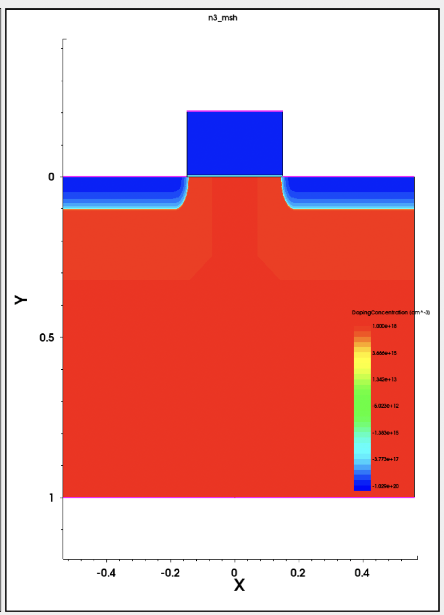
The nMOS device structure was generated using Sentaurus Structure Editor (SDE). The source and drain regions were heavily doped, while the substrate remained lightly doped to form p-n junctions.
Mesh Structure
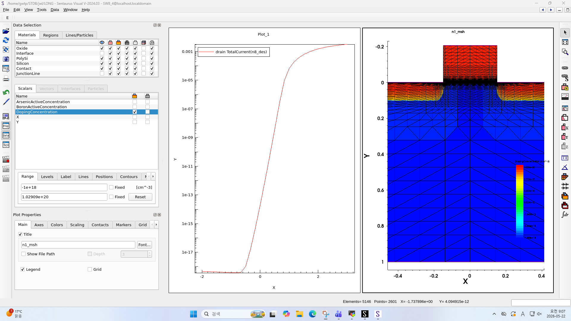
Mesh refinement was applied near the gate oxide and source/drain junctions, where strong electric-field gradients occur. Fine meshing improves numerical accuracy in regions with rapid physical variation.
4. MOSFET Fundamentals
Output Characteristics
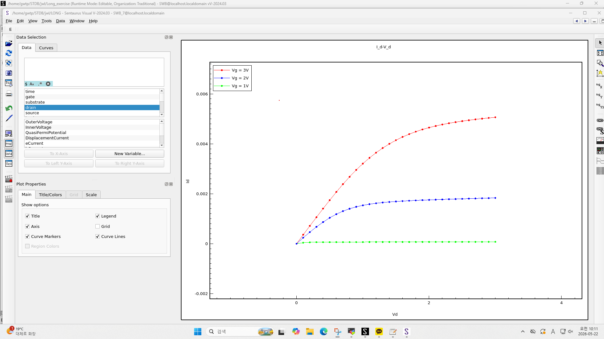
The drain current increases linearly at low drain voltage and gradually enters saturation as the channel approaches pinch-off. Higher gate voltage produces stronger inversion and increases the drain current.
Transfer Characteristics
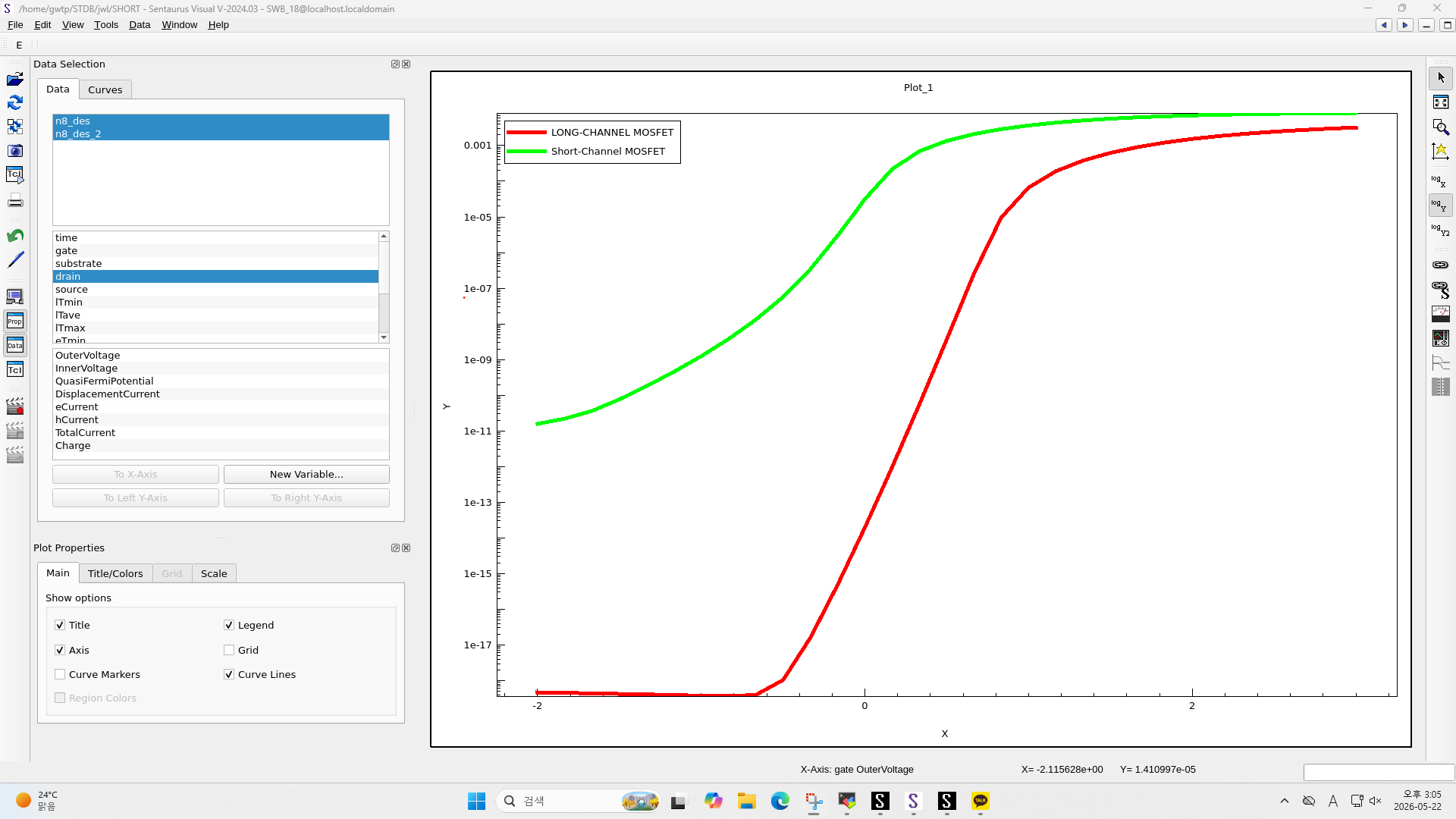
The transfer curve shows the transition from cutoff to strong inversion. Current below the threshold voltage follows exponential behavior, known as subthreshold conduction.
Long-Channel vs. Short-Channel MOSFET
Compared with the long-channel device, the short-channel MOSFET shows larger off-state leakage and degraded gate control. This behavior is caused by stronger drain-channel coupling.
5. Short-Channel Effects
Threshold Voltage Roll-Off
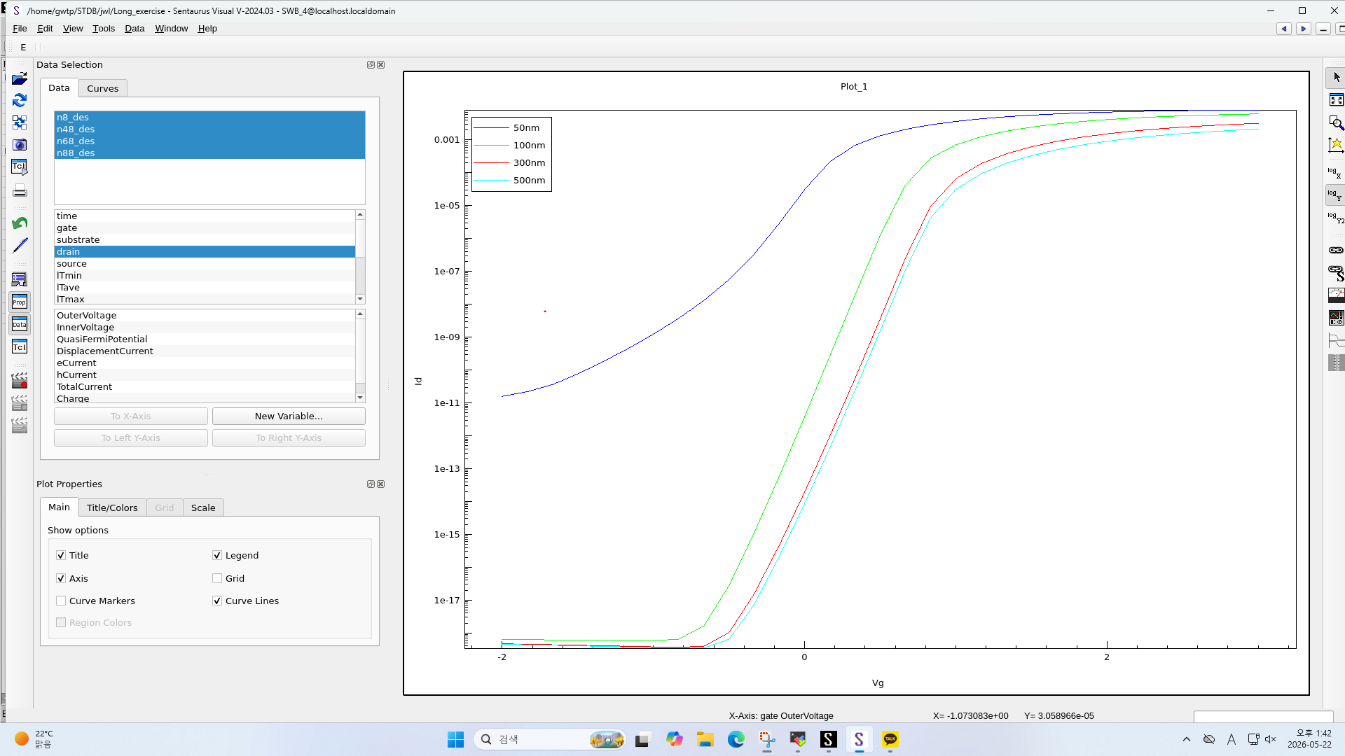
As channel length decreases, threshold voltage decreases due to charge sharing between the source and drain depletion regions. This effect is known as threshold voltage roll-off.
Subthreshold Swing Degradation
The 50 nm device exhibits a more gradual subthreshold slope and higher leakage current. This degradation results from increased short-channel effects and weaker gate control over the channel.
DIBL
Increasing drain bias lowers the source-channel potential barrier and effectively reduces threshold voltage. This phenomenon is known as Drain-Induced Barrier Lowering (DIBL).
Punch-Through
When the source and drain depletion regions merge, carriers can flow directly between the source and drain without sufficient gate control. This leakage mechanism is known as punch-through current.
6. Short-Channel Improvement
LDD Structure
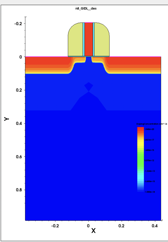
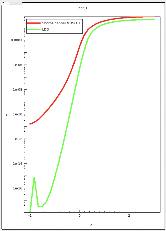
A lightly doped drain (LDD) extension was introduced between the channel and the heavily doped drain region. The LDD device exhibits lower leakage current and improved subthreshold behavior because the drain electric field is distributed over a larger distance, reducing DIBL and hot-carrier effects.
Halo+LDD vs. LDD Implantation
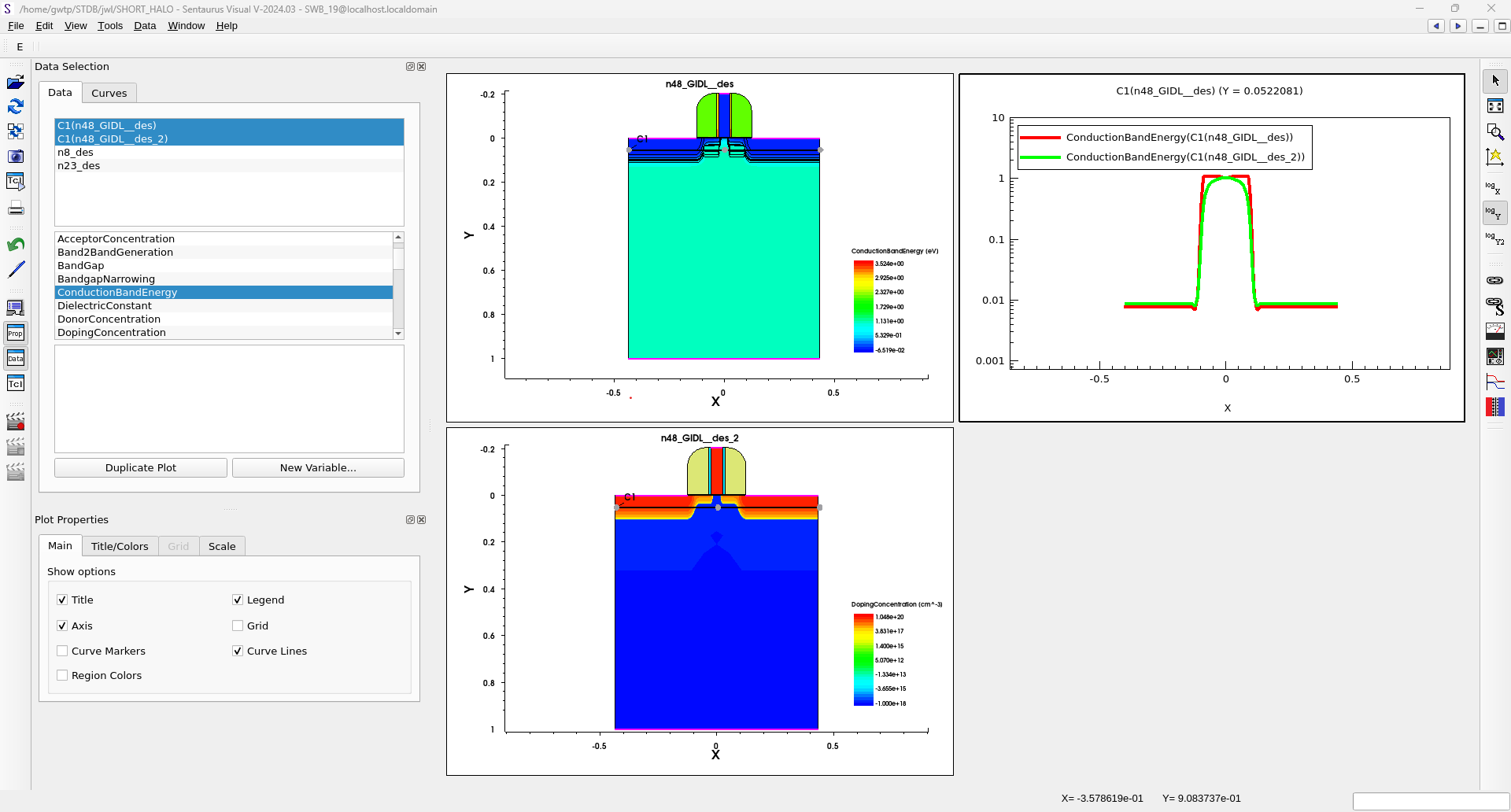
Halo implantation introduces a locally higher body doping concentration near the source and drain junctions. Compared with the LDD-only structure, the Halo+LDD device exhibits a steeper conduction-band profile near the channel edges, indicating stronger electrostatic confinement and improved gate control.
The additional halo doping suppresses depletion-region encroachment from the source and drain, allowing the channel potential barrier to maintain a more abrupt and well-defined shape. As a result, DIBL, punch-through current, and short-channel effects are reduced while subthreshold behavior is improved.
LDD + HALO vs. Short-Channel : Transfer Characteristic Comparison
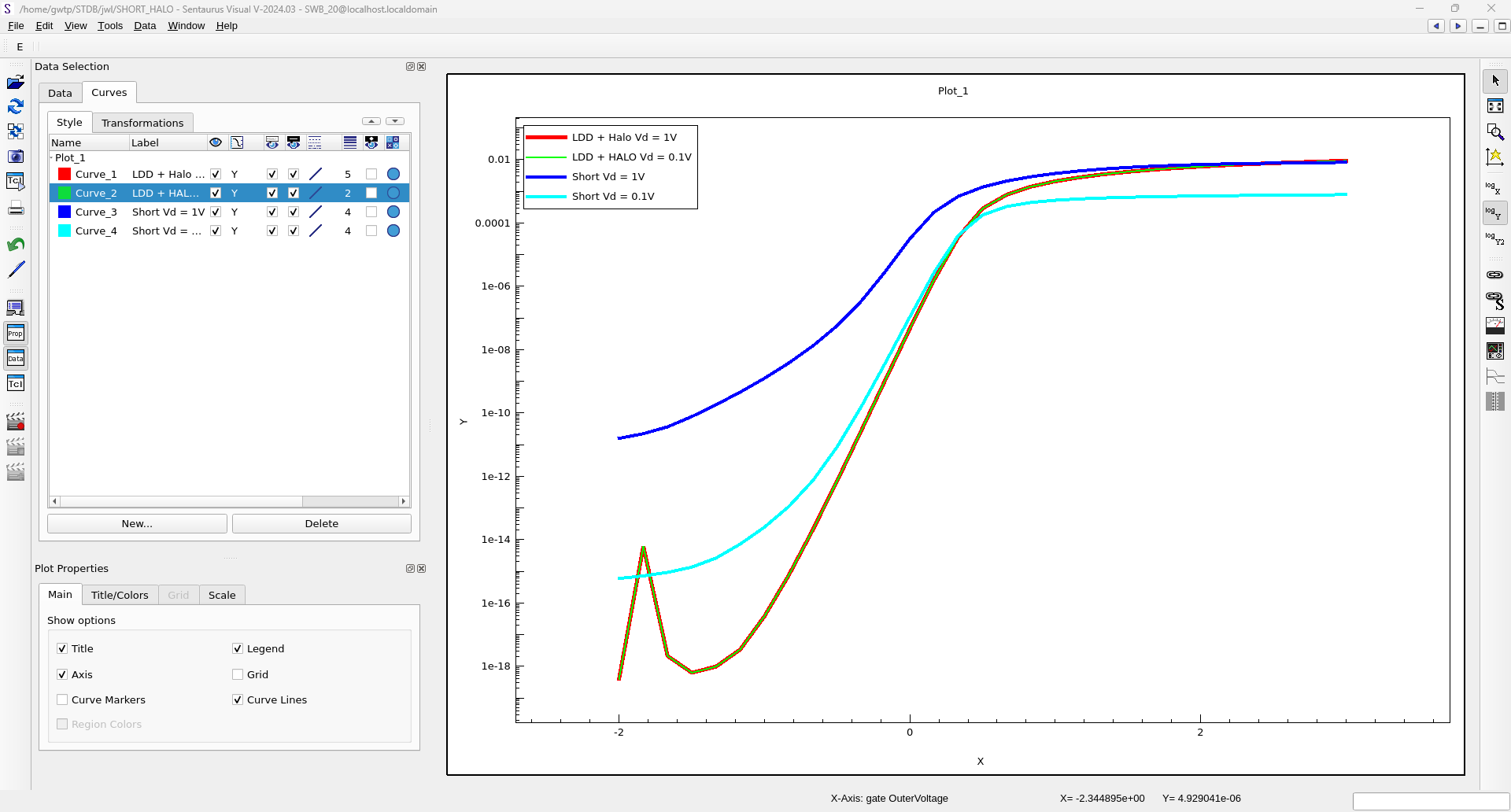
The transfer characteristics of the conventional short-channel MOSFET and the Halo+LDD device were compared under different drain biases. The conventional short-channel device exhibits larger threshold voltage variation and increased off-state leakage as drain voltage increases.
In contrast, the Halo+LDD structure maintains a steeper subthreshold slope and reduced drain-bias dependence. The improved electrostatic control suppresses DIBL and short-channel effects, resulting in lower leakage current and more stable threshold voltage behavior.
7. Gate-Induced Drain Leakage (GIDL)
GIDL Current Characteristics
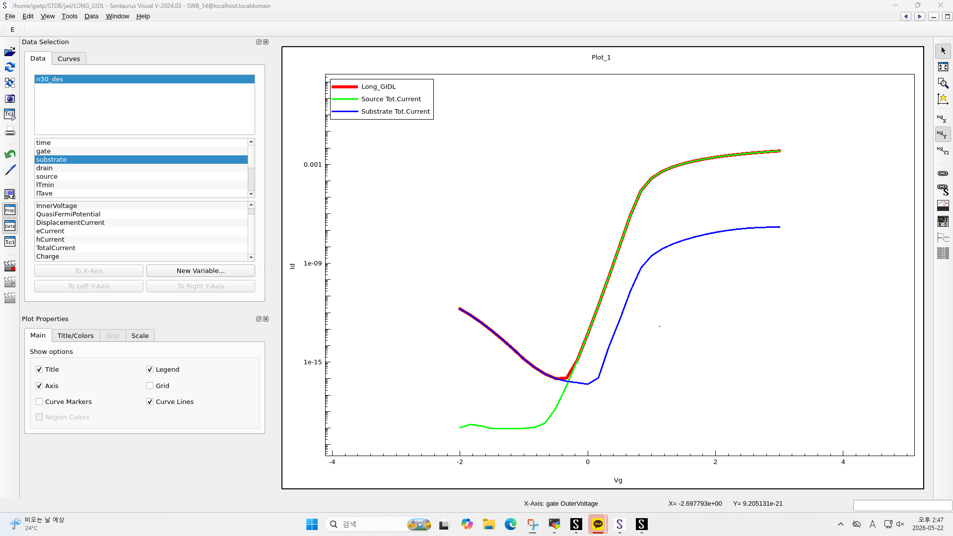
Gate-Induced Drain Leakage (GIDL) was investigated by monitoring the drain, source, and substrate current components during a gate-voltage sweep. Under large negative gate bias, a strong electric field develops near the gate-drain overlap region, inducing band-to-band tunneling and generating leakage current even when the channel remains off.
The drain and source currents represent the resulting leakage path, while the substrate current indicates carrier generation inside the silicon body. The appearance of measurable current under negative gate bias confirms the onset of GIDL leakage caused by high-field tunneling rather than normal channel conduction.
8. SONOS Memory
SONOS Structure and Conduction Band Diagram
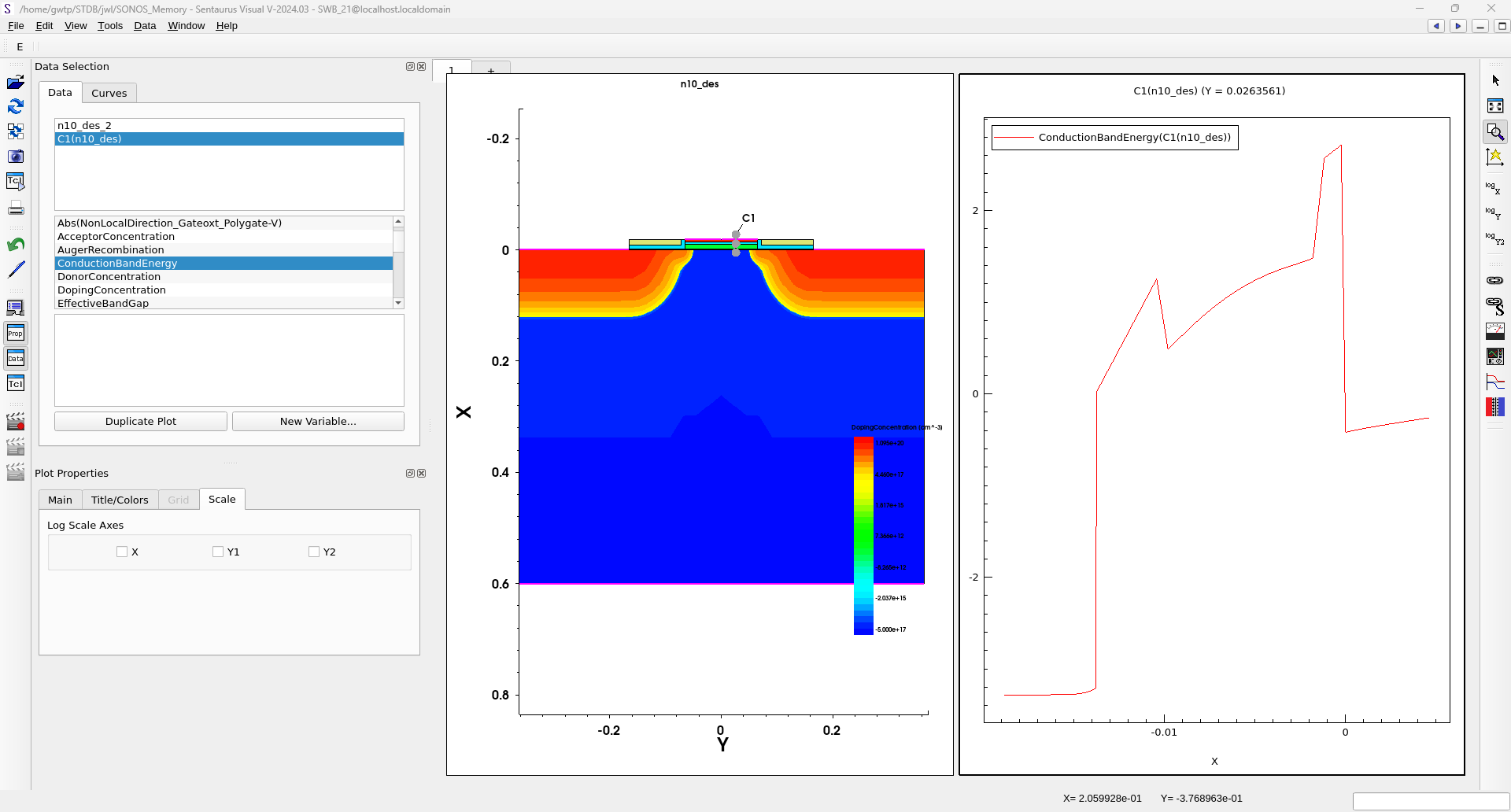
SONOS memory consists of an oxide-nitride-oxide stack, where charge is stored inside the silicon nitride layer. Unlike a floating-gate memory device, SONOS stores charge in localized trap states within the nitride layer.
The conduction-band profile illustrates the tunneling barrier between silicon and the nitride storage layer. Under programming bias, electrons tunnel through the thin oxide layer and become trapped inside the nitride layer.
Programming Operation
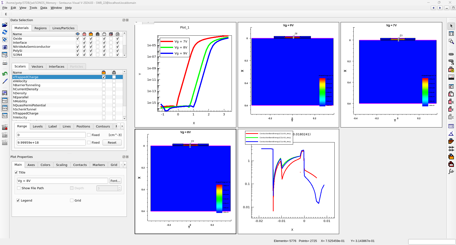
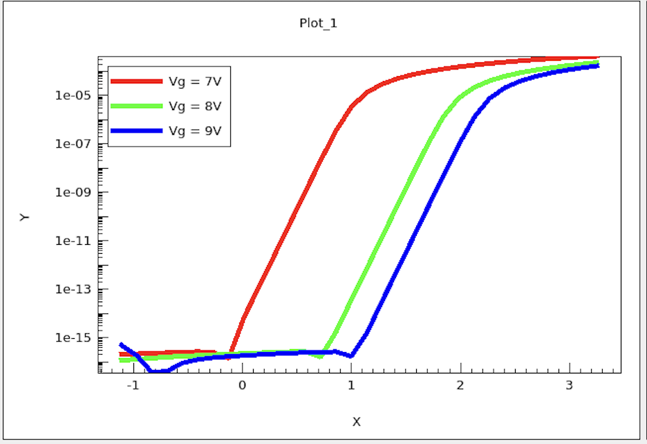
Increasing gate voltage increases electron trapping inside the nitride layer. Higher trapped charge produces a larger threshold voltage shift. The transfer curves shift toward higher threshold voltage as more charge is trapped, representing the programmed memory state.
Erase Operation
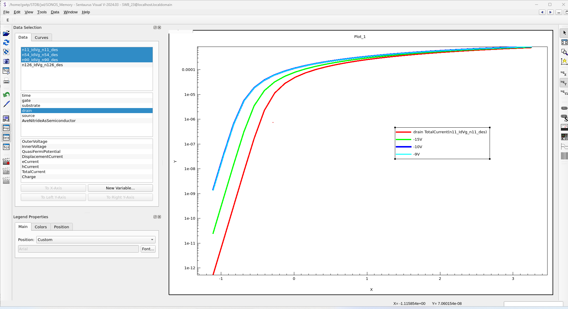
As the erase voltage becomes more negative, more trapped electrons are removed from the nitride layer, resulting in a lower threshold voltage and a stronger erase effect.
However, when the erase voltage becomes excessively large (e.g., -15 V), the strong electric field may induce unwanted charge injection or charge redistribution within the ONO stack, causing the threshold voltage to increase again.
9. CMOS Integration Theory
CMOS fabrication consists of FEOL processes for transistor formation and BEOL processes for interconnect fabrication. FEOL includes oxidation, photolithography, implantation, shallow trench isolation (STI), and well formation. BEOL includes metallization, chemical mechanical polishing (CMP), and interconnect formation.
Reflection
Through TCAD simulation, semiconductor concepts that were previously studied only theoretically became visually observable. In particular, short-channel effects, subthreshold conduction, DIBL, GIDL, and SONOS memory operation were better understood by examining electrical characteristics and physical distributions directly from simulation results.
Project Materials
Certificate of Completion issued by the Korea Semiconductor Training Institute (KSTI). Completed the TCAD Simulation for Nanoelectronic Device Design (Intermediate Level) training program (24 hours).
MOSFET I-V Characteristic Analysis
Completed
Spring 2026
Project Overview
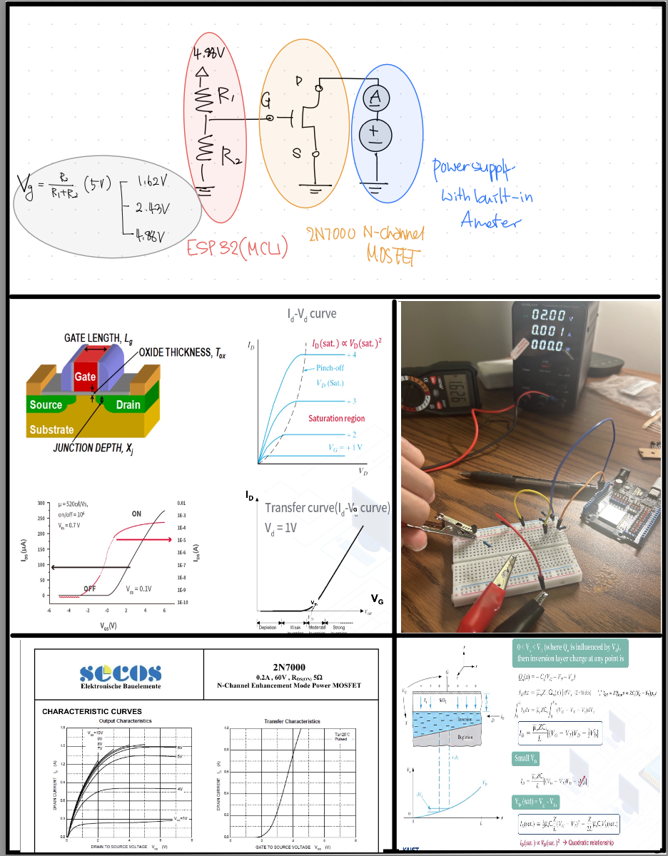
This project focuses on understanding the fundamental physics behind MOSFET operation and experimentally examining its current–voltage (I–V) characteristics. To prepare for the experiment, I studied the theoretical foundations of semiconductor devices, including carrier behavior, energy-band concepts, p–n junction physics, and MOS capacitor behavior under different bias conditions.
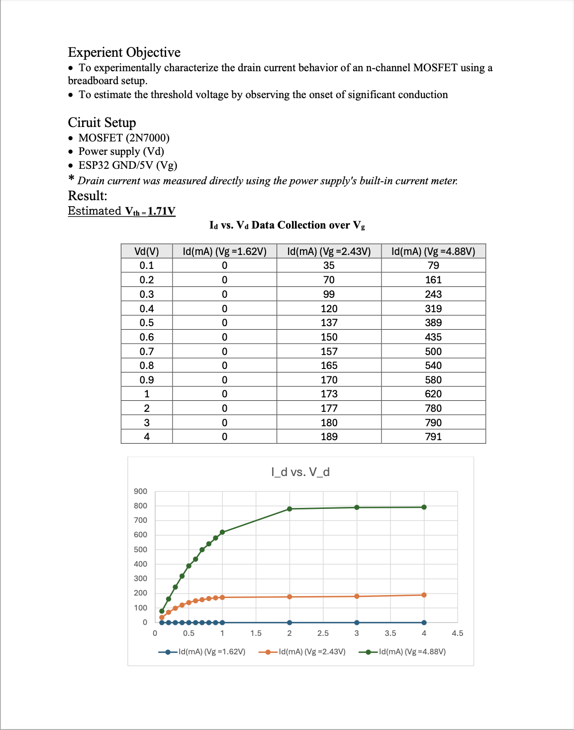
Based on this theoretical background, I built a breadboard setup using an n-channel MOSFET to measure and analyze its I–V characteristics under different gate and drain bias conditions. The project emphasizes connecting device physics theory to practical measurement and data analysis.
My Experience / Project Concept
To prepare for this project, I focused on building a strong theoretical foundation in semiconductor physics. I studied concepts such as crystal lattice structure, energy–momentum (E–k) diagrams, density of states (DOS), Fermi level, and carrier behavior under thermal equilibrium and non-equilibrium conditions.
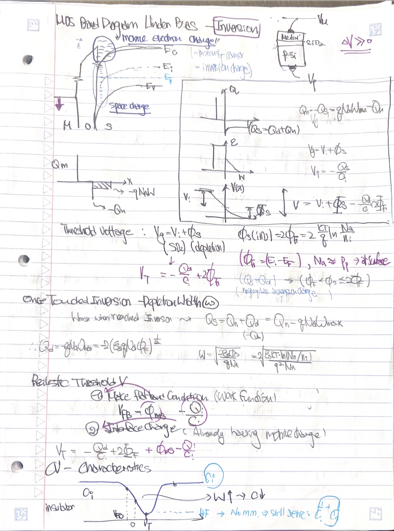
I also studied MOS capacitor physics and band diagram behavior under bias, with particular attention to depletion and inversion conditions. In addition, I explored threshold voltage formation, realistic threshold voltage behavior in practical devices, and current–voltage relationships in the linear and saturation regions of MOSFET operation.
Through this process, I connected theoretical device physics concepts to real experimental measurements by constructing a hardware setup, collecting I–V data, estimating threshold voltage, and analyzing device behavior using plotted measurement results.
One limitation of this project was that the analysis was primarily based on electrical measurements, and I was not able to directly investigate fabrication-related parameters such as mobility, oxide thickness, or channel geometry.
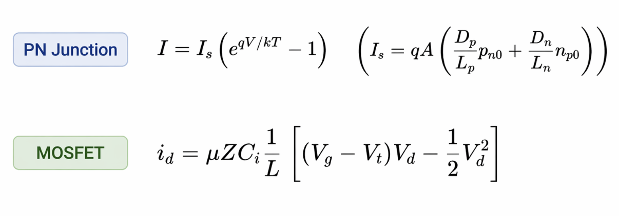
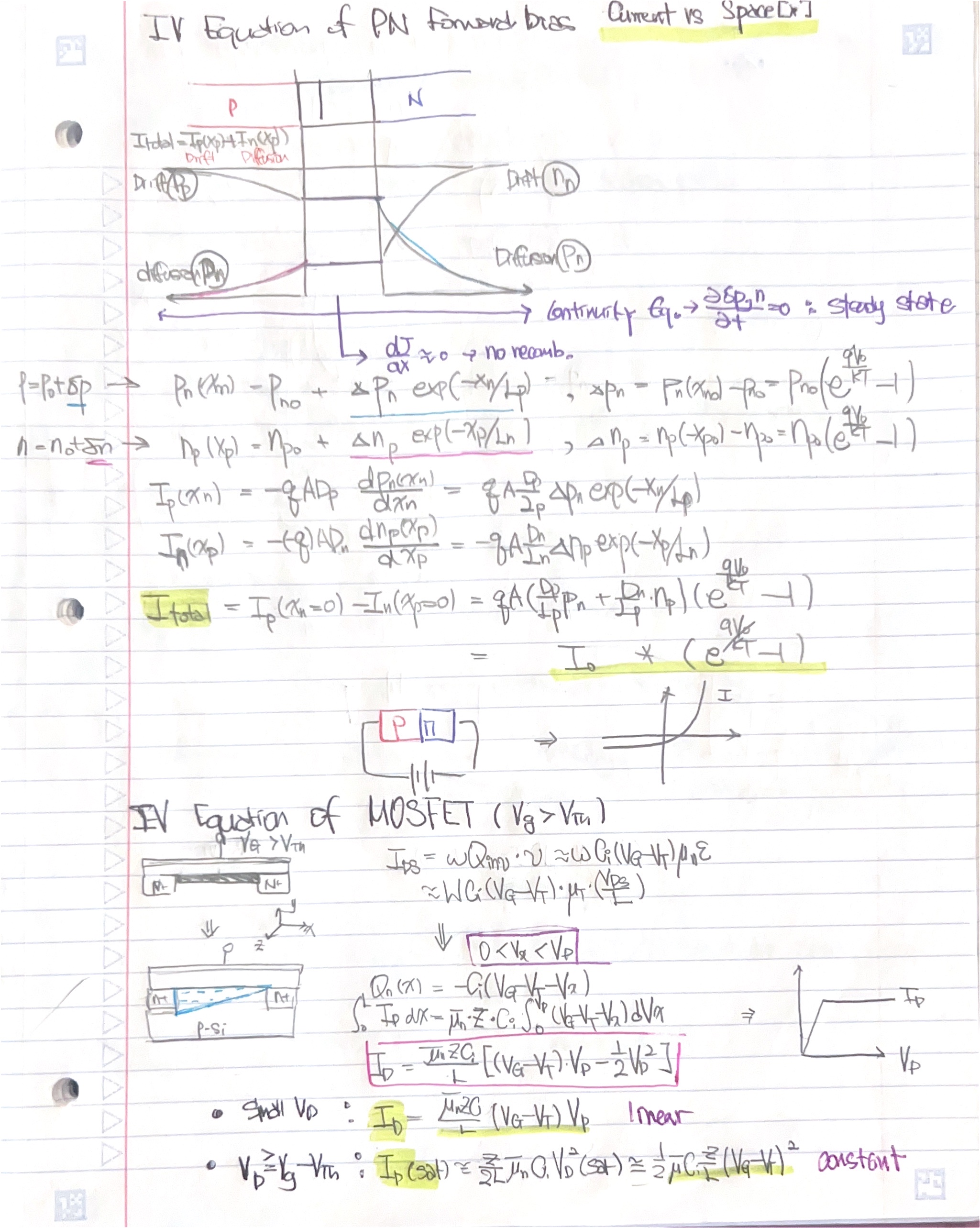
The derivation of I-V equations:
Key Topics and Concepts Applied
- MOS Capacitor Operation and Band Diagram Under Bias
- Inversion Layer Formation and Threshold Voltage
- Realistic Threshold Voltage Estimation from Measured Data
- MOSFET I–V Characteristics (Linear and Saturation Regions)
- Gate Leakage Characteristics (Ig–Vg and Ig–Vd Behavior)
- Breadboard Circuit Implementation and Device Measurement
- Experimental Data Collection and Curve Analysis
Skills
- Semiconductor Device Physics
- MOSFET Operation Principles
- MOS Capacitor and Band Diagram Analysis
- Carrier Transport (Drift and Diffusion)
- Threshold Voltage Extraction from Experimental Data
- Breadboard Circuit Implementation
- Electrical Measurement and Data Analysis
Project Report
Project Materials
Digital Tram Control System Design(FSM)
Completed
Fall 2025
Project Overview
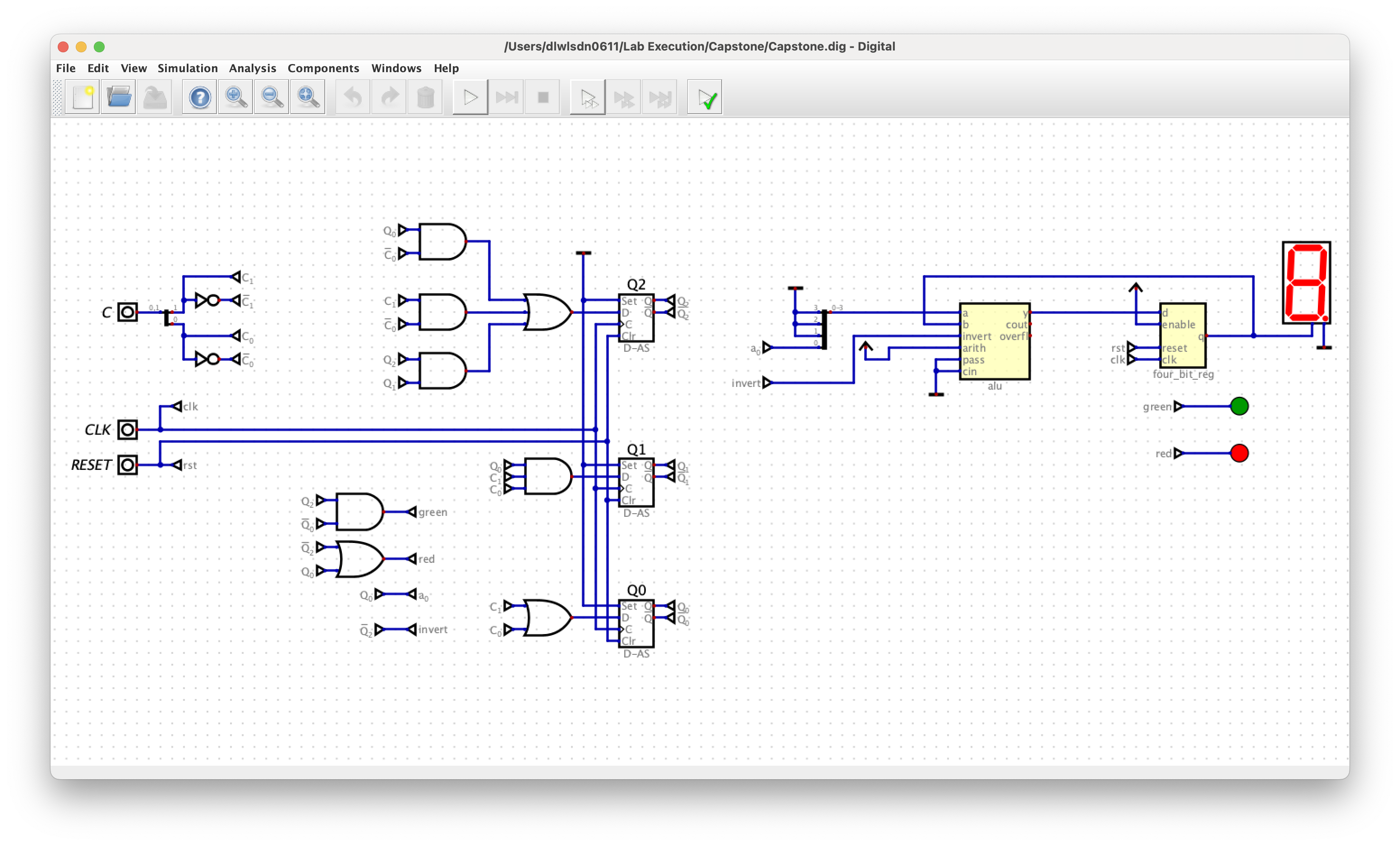
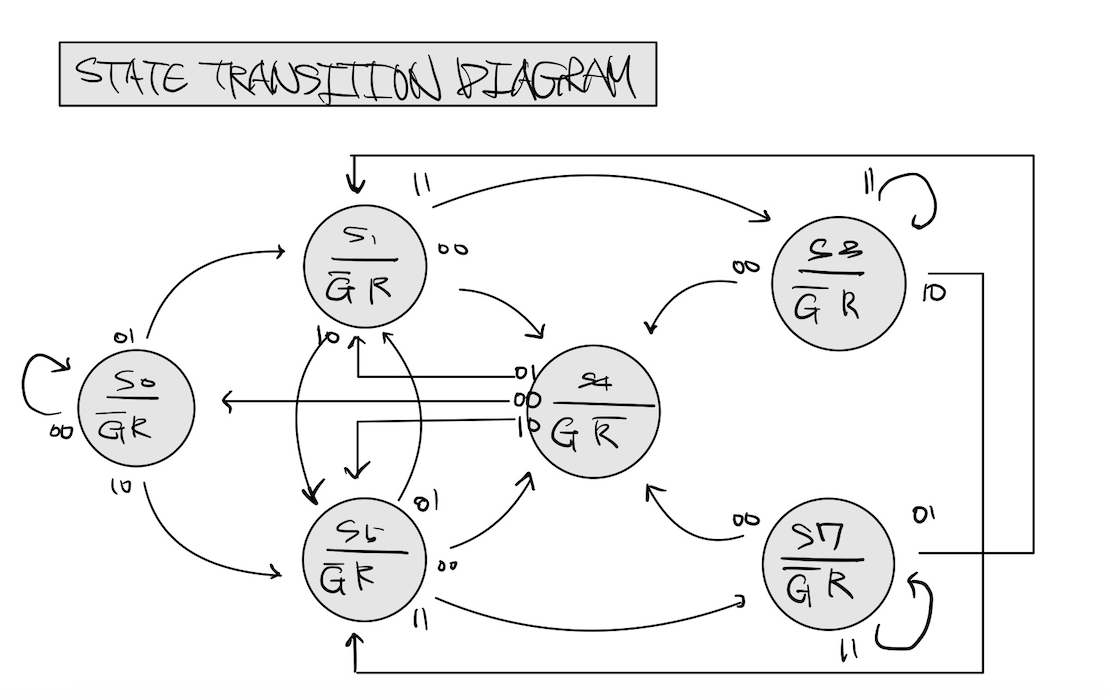
This project involved designing a digital tram control system for an airport transportation setting using a finite state machine (FSM). The client requirement was to create a control system based on four given signals, while the overall FSM structure and implementation strategy were left open-ended. I designed a 6-state tram control system that determines motion and stopping behavior based on the relative progression of states rather than absolute floor position, making the design applicable regardless of the number of stops.
A key objective of my design was hardware minimization. Starting from the state diagram and present-state / next-state relationships, I repeatedly refined the state table and applied Karnaugh map (K-map) minimization to exploit symmetry and repeated logic patterns. By maximizing useful groupings and reducing Boolean expressions, I implemented the system with only 3 D flip-flops, 5 AND gates, 3 OR gates, and 2 NOT gates. The project was verified through digital simulation and received a full score.
My Experience / Project Concept
This project helped me strengthen my understanding of sequential logic design beyond basic FSM construction. I learned how to move from a conceptual control problem to a complete hardware-oriented implementation by building a state diagram, deriving a state table, simplifying logic with K-maps, and validating behavior through simulation. More importantly, I focused on designing the control logic as efficiently as possible rather than only making it function, which gave me stronger insight into digital hardware optimization.
Skills
- Finite State Machine (FSM) Design
- Combinational Logic Design
- Sequential Logic Design
- Karnaugh Map (K-map) Minimization
- Boolean Logic Simplification
- Digital Hardware Design
- Verilog / Digital Simulation
Project Report
Project Materials
Solar Panel Monitoring System
Completed
Aug 2025 – Dec 2025
Project Overview
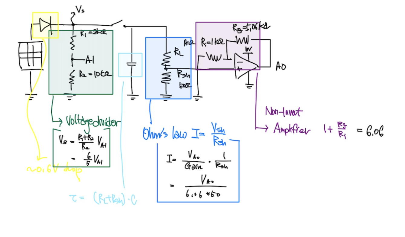
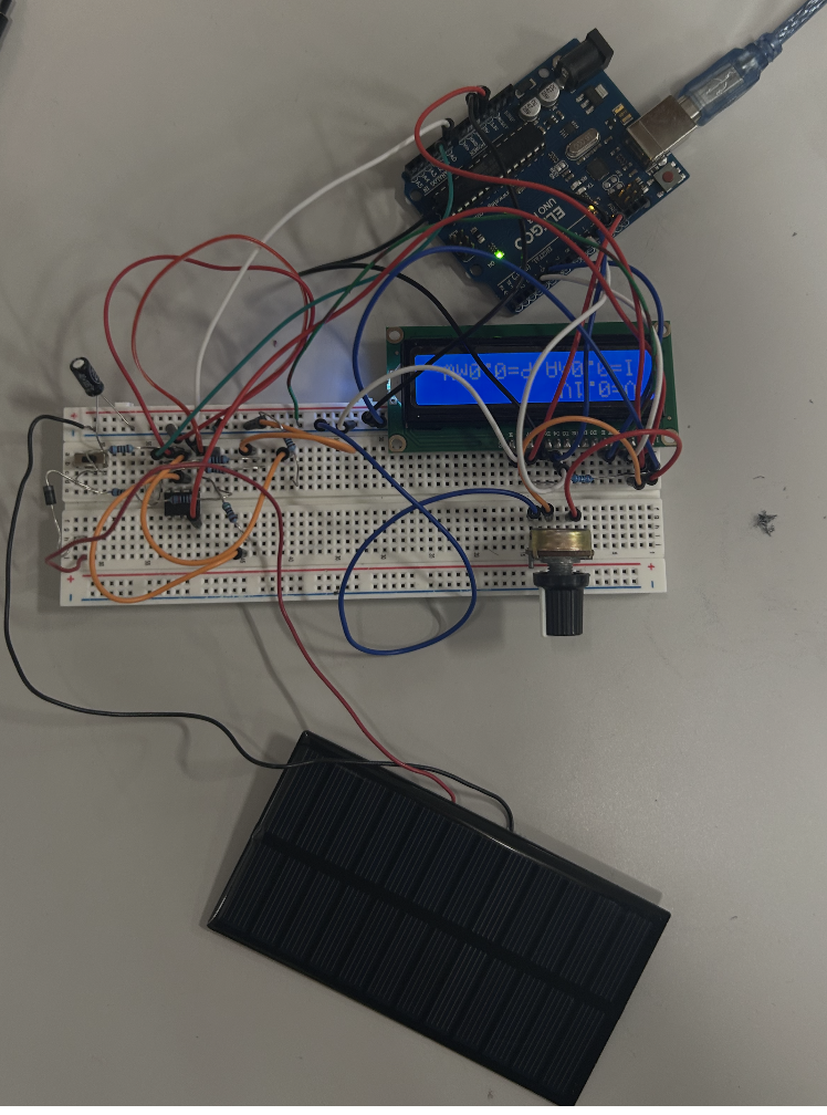
This project involved building a microcontroller-based solar panel monitoring system designed to measure real-time voltage, current, and power from a small-scale solar setup. The system integrated an analog front-end using operational amplifiers, voltage dividers, and a shunt resistor to condition signals for ADC interfacing.
I designed the measurement circuitry, implemented embedded firmware on an Arduino platform, and validated system behavior using laboratory instruments. The project strengthened my understanding of analog signal conditioning, hardware integration, and practical system-level measurement in an embedded environment.
Skills
- Arduino Programming
- Analog Circuit Design
- Operational Amplifier (Op-Amp) Circuits
- Voltage Divider and Shunt Resistor Design
- ADC Interfacing
- Oscilloscope Measurement
- Multimeter Testing
- Embedded System Integration
Project Images
Project Materials
Band-Pass Filter Design & Analysis
Completed
Nov 2024 - Dec 2024
Project Overview
This project focused on the design, theoretical analysis, and experimental verification of a band-pass filter (BPF). The goal was to understand how the circuit passes signals within a specific frequency range while attenuating signals outside that range, and to compare theoretical predictions with measured experimental behavior.
I derived the transfer function in the Laplace domain, analyzed cutoff frequencies, center frequency, and bandwidth, and used Bode plot concepts to interpret the circuit response in the frequency domain. Experimental measurements were then collected and compared with theoretical calculations. The results showed that the measured bandwidth matched the theoretical value closely, while the center frequency showed a larger deviation that was ultimately explained by component tolerances in the resistors and capacitors.
My Experience / Project Concept
This project helped me strengthen my understanding of frequency-domain circuit analysis and the relationship between mathematical modeling and real experimental behavior. I learned how to move from circuit configuration to transfer-function derivation, estimate filter characteristics using theoretical expressions, and interpret discrepancies between theory and measurement. In particular, I gained practical insight into how component tolerances influence the center frequency and overall filter response in real hardware.
Skills
- Band-Pass Filter Analysis
- Laplace-Domain Circuit Analysis
- Transfer Function Derivation
- Bode Plot Interpretation
- Frequency Response Measurement
- Cutoff Frequency / Bandwidth Analysis
- Oscilloscope / PropScope Measurement
- Experimental Data Analysis
Project Images